Image made using the COMSOL Multiphysics® software and is provided courtesy of COMSOL.
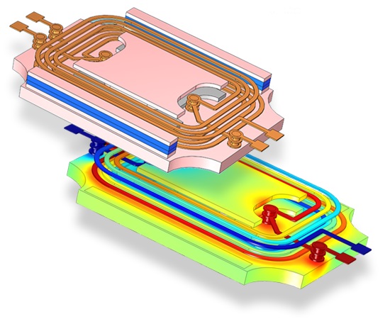
The layout of a planar transformer has been imported from an ECAD file and converted to a 3D geometry model. Shown is the electric potential on its surface.
The development of MEMS devices, integrated circuits (ICs or chips), and printed circuit boards (PCBs) requires greater and greater accuracy in predicting device characteristics and performance, even before manufacturing a prototype. Ever diminishing component sizes demand simulations that incorporate the interactions of several physical phenomena. Using the ECAD Import Module, you can import your ECAD files into COMSOL Multiphysics and convert the 2D layouts into 3D geometry that is suitable for simulation. This opens up a world of simulations, including, among other applications, the electromagnetic, thermal, and structural behavior of these components and devices.
The formats for transferring ECAD data contain the layouts of each layer that makes up a device, whether this is a chip or PCB. The ECAD Import Module will recognize the geometrical shapes on these layouts and construct plane geometry objects that can be extruded according to the layer stack-up information found in the file or provided during import. For MEMS and IC simulation needs, the ECAD Import Module supports the GDSII format. For developing PCBs, the ODB++®, ODB++(X) and NETEX-G file formats can be imported. The NETEX-G format is the native format of a program with the same name, which can be used to extract the connected metal traces for a particular net from Gerber layout and drill files, which are used widely when sending PCB designs for fabrication.
This tutorial model shows how to import data from an ODB++® archive to generate a geometry of a printed circuit board (PCB). Follow the instructions to learn how to remove small details from the geometry, create a mesh, and use automatically generated selections to define physics and mesh settings.
The ODB++® file is provided courtesy of Hypertherm, Inc., Hanover, NH, USA